Enhanced Frequency Doubling Adds to Photonics Toolkit
December 7, 2020
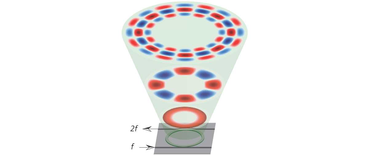
A new photonic chip can double the frequency (f) of incoming light using a circular ring 23 microns across. The ring is tailored to generate and hold light at the input frequency and at its second harmonic (2f)—just like piano strings or organ tubes can host harmonics of a single tone. The color indicates crests and troughs of the light field, similar to a piano string’s displacement pattern when it rings. (Credit: Xiyuan Lu/NIST and UMD)
The digital age has seen electronics, including computer chips, shrink in size at an amazing rate, with ever tinier chips powering devices like smartphones, laptops and even autonomous drones. In the wake of this progress, another miniature technology has been gaining steam: integrated photonics.
Photons, which are the quantum particles of light, have some advantages over electrons, the namesakes of electronics. For some applications, photons offer faster and more accurate information transfer and use less power than electrons. And because on-chip photonics are largely built using the same technology created for the electronics industry, they carry the promise of integrating electronics and photonics on the same chip.
Tiny photonic chips have already been adopted in many places, including telecommunications networks (think fiber optic internet) and large data centers (think interfacing fiber-optics with electronics). Other industries are on the precipice of benefitting from photonics, with self-driving car makers developing light-based radar chips. However, many tools that are well-established in traditional optics—things that use lasers, lenses and other bulky equipment—do not yet have a compact photonic analogue. For futuristic tools like light-based quantum computers or portable optical clocks, more work remains to package everything together.
Now, researchers at JQI have added a new tool to the photonics toolkit: a way to use silicon, the native material for much of digital electronics and photonics, to efficiently double the frequency of laser light. By combining two existing techniques, the team achieved a frequency doubling efficiency 100 times greater than previously experiments with silicon compounds. They detailed their results in a paper published in the journal Nature Photonics.
Light waves are made up of photons, but they also carry a frequency. Our eyes see a small fraction of these frequencies as the colors of the rainbow, but microwaves, x-rays and radio waves (among others) also inhabit this spectrum. Doubling the frequency of light is one way to convert between these different ranges. In the new work, the team demonstrated a doubling of infrared light—commonly used in optical telecommunications—to red light, the language of very precise atomic clocks.
Frequency doubling is one effect that can occur when light interacts with the medium it’s traveling through, be it air, water or silicon. Depending on the properties of these materials, a little bit of the light can be doubled, tripled, or, in extreme cases, multiplied to even higher degrees, like a musical note also generating a bit of sound one, two, or several octaves up. By choosing the right material, and illuminating it in the right way, researchers can get to the harmonic they need.
Unfortunately, silicon and silicon compounds—the materials of choice for routing light on a chip because of the maturity of silicon manufacturing and the ease of integrating with electronics—don’t intrinsically support frequency doubling. The crystal structure is too uniform, meaning it looks the same in all directions. This prohibits the doubling effect, which relies on electrons in the material shifting one way more than another under the influence of light. But once light is confined to a tiny trace on a chip, things become a little less uniform: After all, the air is always nearby, and it doesn’t look at all like a silicon crystal. So, a tiny amount of frequency doubled light does get generated, but usually it is not enough to be useful.
In the new work, a team led by JQI Fellow Kartik Srinivasan, a Fellow of the National Institute of Standards and Technology (NIST), and NIST and UMD postdoctoral researcher Xiyuan Lu, combined two previously explored techniques to build on this tiny effect, generating 100 times more frequency doubled light than any previous silicon experiments. Additionally, their doubling occurred with an efficiency of 22%, appreciable enough to be useful in applications.
The first trick was to capture the light in a resonator, making the light go round and round and triggering the tiny doubling effect over and over again. To achieve this, the researchers first routed near-infrared laser light into an optical fiber. The fiber then shot the light into a silicon nitride waveguide printed on a silicon chip. This waveguide led to another waveguide, which was wrapped into a circle just 23 microns in diameter. The circular resonator, which was engineered to capture the incoming light and circulate it around, allowed a tiny bit of frequency doubling to happen over and over again. Another straight waveguide, on the other edge of the resonator, was tuned to carry away the frequency-doubled light.
The second trick was to make the silicon less uniform by biasing it with an electric field. Luckily, no external field was actually needed—the tiny amount of frequency doubled light, combined with the original infrared pump light, caused the electrons in the resonator to gather at the edges, creating a constant electric field. This field greatly enhanced the frequency doubling capacity of the silicon nitride.
“It’s a feedback process,” says Srinivasan, “because a little bit of frequency doubled light and pump light start to create the constant electric field, making the frequency doubling process stronger, which in turn creates more frequency doubled light. So both the pump light and the frequency doubled light are circulating around in this ring, and there’s this huge ability to take this thing that started out as extremely weak, and then actually make it a pretty strong effect.”
Getting both of these effects to work in the same device wasn’t easy. Not only does the resonator ring need to be exactly the right size to trap the pump and frequency doubled light, the light also needs to stack up in the right way in the resonator. To achieve this, detailed simulations and precise manufacturing in a clean room are necessary. But once such an accurate device is fabricated, all you need to do is send in pump light, and observe frequency doubled light at the output.
“To enable efficient interaction between light and the material, light of different colors has to live a long time and also move at exactly the same speed,” says Lu, “Our device implements these two key factors into photo-induced frequency doubling, which significantly boosts the power efficiency of this process.”
This device is another step in a long quest to achieve a portable, ultra-precise atomic clock. “These optical clocks are these amazing timekeeping devices, but usually they're in a big lab,” says Srinivasan. “If it could be in a small package it could go on cars or drones or other vehicles. Timing underlies a lot of important navigation applications, and for the most part, now, people rely upon GPS signals. But there are all sorts of possibilities that there might be something in the way, and you can’t acquire those signals, or somebody spoofs the signal. So, having portable timing instruments that could really give you accurate and precise time for long stretches before you need a synchronization signal from GPS is meaningful.”
Although it’s not the star of the show, frequency doubling is a necessary component in optical atomic clocks. These clocks produce an extremely regular beat, but at optical frequencies—hundreds of trillions of light field oscillations per second. Conventional electronics can’t interface with that signal directly, so to bring this precision down to an intelligible frequency (mere billions of oscillations per second) scientists use frequency combs—laser sources with frequency ‘teeth’ at perfectly regular intervals, an invention that won the 2005 Nobel Prize in physics.
To be useful, these frequency combs need to be calibrated—each tooth in the comb needs to be labeled with a specific frequency value. The simplest and most common way to calibrate them is to take the lowest tooth in the comb, frequency double it, and compare to the highest tooth: this gives the frequency of the lowest tooth. Along with a simple measurement of the spacing between teeth, scientists can use this to deduce the exact frequency of each tooth.
Recently, several pieces of the on-chip atomic clocks, including tiny atomic vapor cells and on-chip frequency combs, have been achieved in silicon-based photonics. However, the frequency doubling calibration was previously done with bulky optics or using materials that are less compatible with silicon. “At least conceptually,” says Srinivasan, “we’re one step closer to a calibrated frequency comb in a really compact package. There's still work to be done to really be able to put these things together, but we’re closer to a compact optical atomic clock than we were before.”
Story by Dina Genkina
In addition to Srinivasan and Lu, this paper had 3 additional co-authors: Gregory Moille, a postdoctoral researcher at JQI and NIST; Ashutosh Rao, a postdoctoral researcher in chemistry and biochemistry at UMD and NIST; and Daron A. Westly, a research scientist at NIST.
Experts
People
![a photo of a man wearing a blue and white checked shirt in front of greenery]()
Kartik Srinivasan
Adjunct Professor, JQI Co-Director
![Xiyuan Lu]()
Xiyuan Lu
Assistant Research Scientist
Groups
JQI

